• Home
  • About Us
    • Mission and History
    • Meet Our Team
  • Flip Chip Bonders
    • ACCµRA™ M
    • ACCµRA™ OPTO
    • ACCµRA™100
    • ACCµRA™ Plus
    • FC150 PLATINUM
    • FC300
    • LDP150
  • Atmospheric Plasma
    • ONTOS CLEAN
    • Atmospheric Plasma – OntosIS (OEM)
  • Delta Printing System
  • Other Products
    • MagVision Kerr Imaging System
    • AST IR Imaging Microscopes
  • Events & Technical Papers
    • Conferences / Exhibitions
    • C2W Hybrid Bonding Consortium
    • TP: Die Bonders
    • TP: Atmospheric Plasma
  • Contact Us

Call us today! +1 (603) 548-7870

Find our Location
[email protected]
Login

Login
SetnaSetna
SetnaSetna
  • Home
  • About Us
    • Mission and History
    • Meet Our Team
  • Flip Chip Bonders
    • ACCµRA™ M
    • ACCµRA™ OPTO
    • ACCµRA™100
    • ACCµRA™ Plus
    • FC150 PLATINUM
    • FC300
    • LDP150
  • Atmospheric Plasma
    • ONTOS CLEAN
    • Atmospheric Plasma – OntosIS (OEM)
  • Delta Printing System
  • Other Products
    • MagVision Kerr Imaging System
    • AST IR Imaging Microscopes
  • Events & Technical Papers
    • Conferences / Exhibitions
    • C2W Hybrid Bonding Consortium
    • TP: Die Bonders
    • TP: Atmospheric Plasma
  • Contact Us

SEMICON Europe 2025, Nov. 18-21, Munich, Germany

Home » SEMICON Europe 2025, Nov. 18-21, Munich, Germany

SEMICON Europe 2025, Nov. 18-21, Munich, Germany

May 5, 2025 Posted by Setna Latest News

SEMICON-Europa

Meet our sister company ONTOS on Booth C2-433 to discuss the Atmospheric Plasma ONTOS CLEAN and its OEM Version ONTOS IS

Exhibition hours:

  • 9:00am to 6:00pm on Tuesday, November 18.
  • 9:00am to 6:00pm on Wednesday, November 19.
  • 9:00am to 6:00pm on Thursday, November 20.
  • 9:00am to 4:00pm on Friday, November 21.

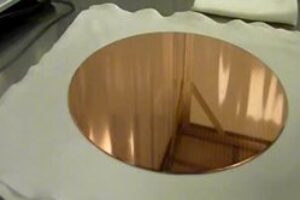
Surface Preparation with Ontos Atmospheric Plasma

We shall be pleased to discuss the Advantages of our Atmospheric Plasma ONTOS CLEAN for Surface Preparation. It is applicable to numerous process steps for Semiconductor Manufacturing or Assembly.

ONTOS IS  is also available as an OEM version which can be integrated into production machines.

Applications include:

  • Photoresist de-scum & activation,
  • Preparation for plating,
  • Photomask cleaning,
  • Bonding (de-oxidation, protection against re-oxidation),
  • Preparation for Capillary underfill,
  • Surface activation for adhesive bonding.

Share
0

About Setna

SETNA is a Manufacturing and Marketing, Sales and Service Organization. It is centered on our experience and know-how in high-accuracy bonding and the equipment, materials, competencies surrounding it including Surface Preparation with Atmospheric Plasma. SET Bonders have been the world-standard for applications in which micron precision post bond accuracy is required.

You also might be interested in

SEMICON West | October 7-9, 2025 | Phoenix AZ, USA

SEMICON West | October 7-9, 2025 | Phoenix AZ, USA

May 5, 2025

SEMICON-West – Meet us on SET Corporation booth #557 Venue: Convention[...]

Copper Plating

Comparison of Ontos7 Treated and Un-Treated Cu Plating Base

Jun 8, 2014

Movie showing the significant improvement of the wetting after Atmospheric[...]

Ontos 7 Treated SAC bumps on Si Chip

Ontos 7 Treated SAC bumps on Si Chip

Jun 8, 2014

This video is showing the Wetting Improvement provided by the[...]

Contact Us:


    Contact Us:

    • Setna, LLC
    • 343 Meadow Fox Ln, Chester, NH 03036
    • +1 (603) 548-7870
    • sales@set-na.com

    Technical Papers Quick Links:

    • Atmospheric Plasma
    • Die Bonders

    Information about SET Bonders:

    SET – Smart Equipment Technology, is the leading supplier of high accuracy Die-to-Die and Die-to-Wafer bonders.

    Visit set-sas.fr.

    Information about OES Plasma:

    ONTOS Equipment Systems, a sister company founded by SETNA, is a manufacturer of innovative devices for surface activation using room-temperature plasma.

    Visit ontosplasma.com.

    © 2025 — Setna, LLC

    • Home
    Prev Next