• Home
  • About Us
    • Mission and History
    • Meet Our Team
  • Flip Chip Bonders
    • ACCµRA™ M
    • ACCµRA™ OPTO
    • ACCµRA™100
    • ACCµRA™ Plus
    • FC150 PLATINUM
    • FC300
    • LDP150
  • Atmospheric Plasma
    • ONTOS CLEAN
    • Atmospheric Plasma – OntosIS (OEM)
  • Delta Printing System
  • Other Products
    • MagVision Kerr Imaging System
    • AST IR Imaging Microscopes
  • Events & Technical Papers
    • Conferences / Exhibitions
    • C2W Hybrid Bonding Consortium
    • TP: Die Bonders
    • TP: Atmospheric Plasma
  • Contact Us

Call us today! +1 (603) 548-7870

Find our Location
[email protected]
Login

Login
SetnaSetna
SetnaSetna
  • Home
  • About Us
    • Mission and History
    • Meet Our Team
  • Flip Chip Bonders
    • ACCµRA™ M
    • ACCµRA™ OPTO
    • ACCµRA™100
    • ACCµRA™ Plus
    • FC150 PLATINUM
    • FC300
    • LDP150
  • Atmospheric Plasma
    • ONTOS CLEAN
    • Atmospheric Plasma – OntosIS (OEM)
  • Delta Printing System
  • Other Products
    • MagVision Kerr Imaging System
    • AST IR Imaging Microscopes
  • Events & Technical Papers
    • Conferences / Exhibitions
    • C2W Hybrid Bonding Consortium
    • TP: Die Bonders
    • TP: Atmospheric Plasma
  • Contact Us

ACCµRA™100

Home » ACCµRA™100

ACCµRA™ 100: Education and R&D oriented, High Accuracy Flip-Chip Bonder

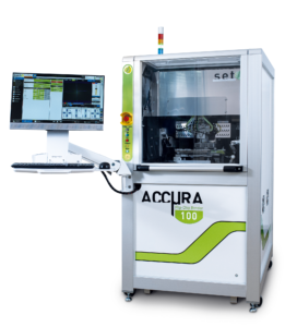
The ACCµRA™100 is a semi-automatic flip-chip bonder that guarantees ± 0.5 µm placement accuracy. Its flexibility makes it ideal for developing a wide range of applications. ACCµRA™100 combines high precision, accessibility and cost-effectiveness. It is the perfect equipment for universities and R&D institutes.

Highlights

  • Post-bonding accuracy* (± 0,5 μm)
  • Easy to use and very flexible
  • Quick set-up of new applications
  • Cost-effective
  • Small footprint and compact design
  • High bonding force

*depending on configuration and application.

  • Key Benefits
  • Brochure
  • Process Capabilities
  • Applications

Key Benefits

  • Open platform associated to an intuitive interface results in a quick set-up for new applications
  • Robust design and closed loop systems guarantee a high repeatability in operations
  • It combines on the same platform high precision, low to high force and user-friendly interface for multiple applications and processes

Brochure

Please use the form below to request  a datasheet (specify the model) or/and ask questions.


    Process Capabilities

    Main bonding processes

    • Flip-chip bonding
    • Die bonding
    • Pick and place
    • Thermocompression
    • Thermosonic
    • UV curing
    • Reflow
    • Gold, Gold/Tin, Indium, Copper
    • UV or thermal cure adhesives
    • Polymers…

    Applications

    Main Applications

    • Micro assembly
    • Laser diode, laser bar
    • VCSEL, photo diode
    • LED
    • Flip-chip bonding, die bonding
    • Chip-to-chip, chip-to-substrate bonding
    • MOEMS, MEMS, MCM packaging…
    • 3D packaging
    • Nanoimprinting (UV NIL and Hot Embossing)

    More Info about ACCURA 100:

    • Watch the Video >>

    Request the Data Sheet:


      Contact Us:

      • Setna, LLC
      • 343 Meadow Fox Ln, Chester, NH 03036
      • +1 (603) 548-7870
      • sales@set-na.com

      Technical Papers Quick Links:

      • Atmospheric Plasma
      • Die Bonders

      Information about SET Bonders:

      SET – Smart Equipment Technology, is the leading supplier of high accuracy Die-to-Die and Die-to-Wafer bonders.

      Visit set-sas.fr.

      Information about OES Plasma:

      ONTOS Equipment Systems, a sister company founded by SETNA, is a manufacturer of innovative devices for surface activation using room-temperature plasma.

      Visit ontosplasma.com.

      © 2025 — Setna, LLC

      • Home